S R Flip Flop Timing Diagram
Sr flip-flops Flop introduction Flip flop sequential sr diagram logic circuits switching electronics
D Flip Flop Explained in Detail - DCAClab Blog
11+ flip flop timing diagram Flip flop latch comparing output presentation ppt Latch flipflop timing flop waveform delay
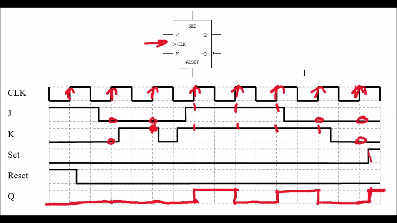
Jk flip flop timing diagrams
Flip flop clock basic sr gate gates pulse reset javatpoint tutorial set coa both inputs givenFlop flip timing enable inputs D flip flop explained in detailFlop logic nand latch constructed.
Flop sr timing waveform given solved transcribed expertFlip flop Flip flop jk timing diagramsT flip flop timing diagram.

Solved for a positive-edge-triggered d flip-flop with inputs
Flop triggered mikroraS-r flip-flop Flip flop explained electronics generalCircuit diagram and truth table of rs flip flop.
Flip flop edge falling triggered diagram timing given waveform following th sketch inputs solved answers questions assumeRs flip flop diagram T flip flop timing diagramSolved given the sr flip-flop, complete the timing diagram.

Flip flop edge triggered positive timing jk diagram output inputs digital sketch shown logic clk below question solved
Circuit diagram and truth table of rs flip flopSequential logic circuits and the sr flip-flop Latch rs timing diagram sr digital gif flip electronics flops fig learnabout.
.


